Chapter 27 - Let’s make our own PCB #
Printed Circuit Borads look like something reserved for only big business, but that is very much so not the case. It’s suprisingly cheap to get smaller boards made, espically if you’re okay with waiting a week or two on international shipping. But, let me back up- what even is a PCB?
Well, when anyone first starts with circuits, they go for the ever popular breadboard:
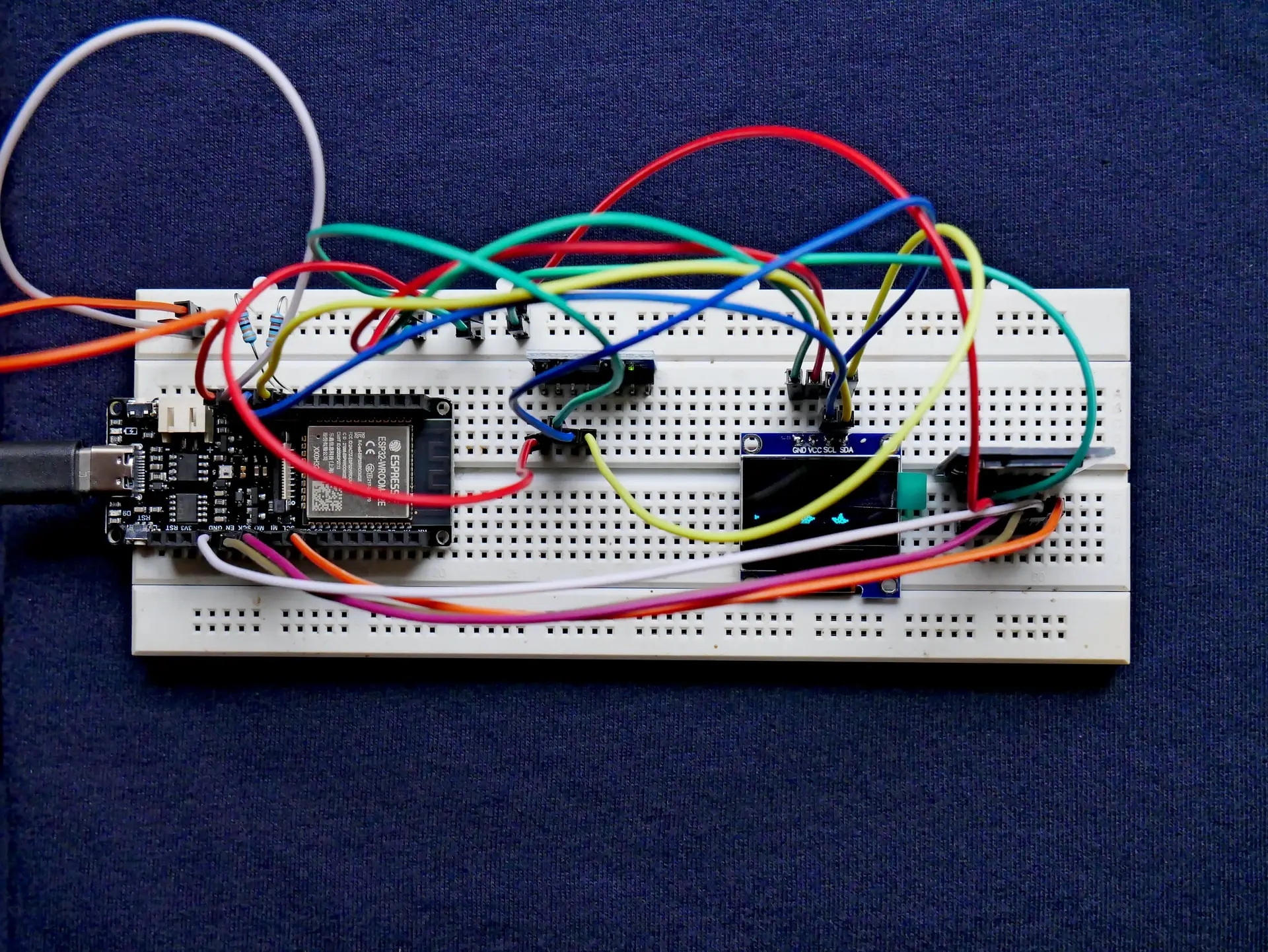
Image by Vishnu Mohanan
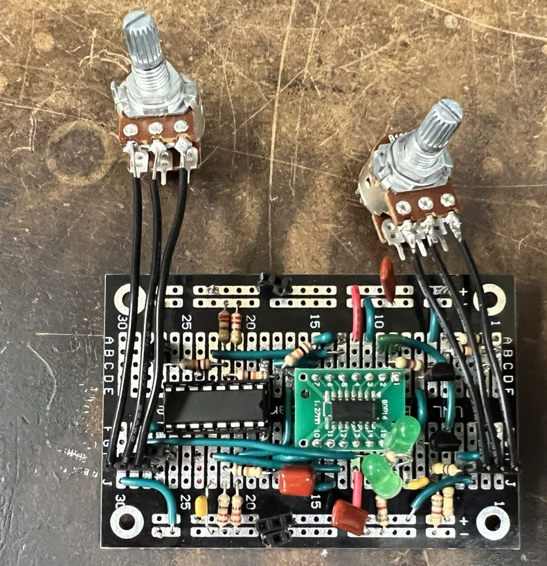
Then, you may decide to make a more reliable version, soldered together on a perma-proto board:
But ultimately, the best, most reliable way to build your circuit is with a PCB:
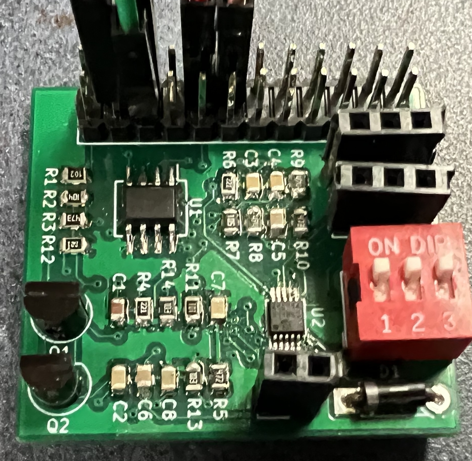
In case it’s not obvious, these three images are not of the same circuit. So, you can’t directly compare complexity between these images.
Now, there’s a few things you should notice about the version on the PCB:
- It’s a hell of a lot more compact
- The wiring is all part of the board - it’s very difficult to correct a mistake at this point
- But it’s more reliable, no risk of a lose wire or bad contact like in the breadboard
- The parts are much smaller
- This isn’t required - you could use the same, through-hole parts, but generally these Surface Mount Device (SMD) components that you see are actually easier to work with and, due to their small size, keep cost down
So, how do you make one? Well, software is needed obivously. For that, there’s many options but for most people the free and open source tool KiCad will do everything you need. So, go grab the latest version of it from https://www.kicad.org or your repos if you’re using Linux. Get that installed. Then, go ahead and watch this video which does a better job of explaining things quickly than I possibly could in text:
Sorce: Foalyy @ https://forum.kicad.info/t/cheatsheet-for-kicad/5247
[TODO] - pick a PCB design to walk though making on this page - maybe an APC?
- PCB specic things - Layers, Vias, fills, silk, mask, 0-ohm resistors,
- Make it work
- Make it not emit a ton of RF or go to shit when around it (everything is an antenna)
- Make it pretty
- ref that weird russian autorouter as limits on this
- Make it repairable
- Pretty + Repairable means we need good, well labled silkscreen, componet spacing, etc.
- Know when to do a PCB or a Perma-Proto
- Assuming parts will only be available for so long
- Do not assume same package = same pinout
- Do not assume a sane pinout, even in a device family. The tab can be anything!
- Expect to need to order a 2nd time
https://llllllll.co/t/pcb-art-artfully-shaped-copper-traces/22027/2t
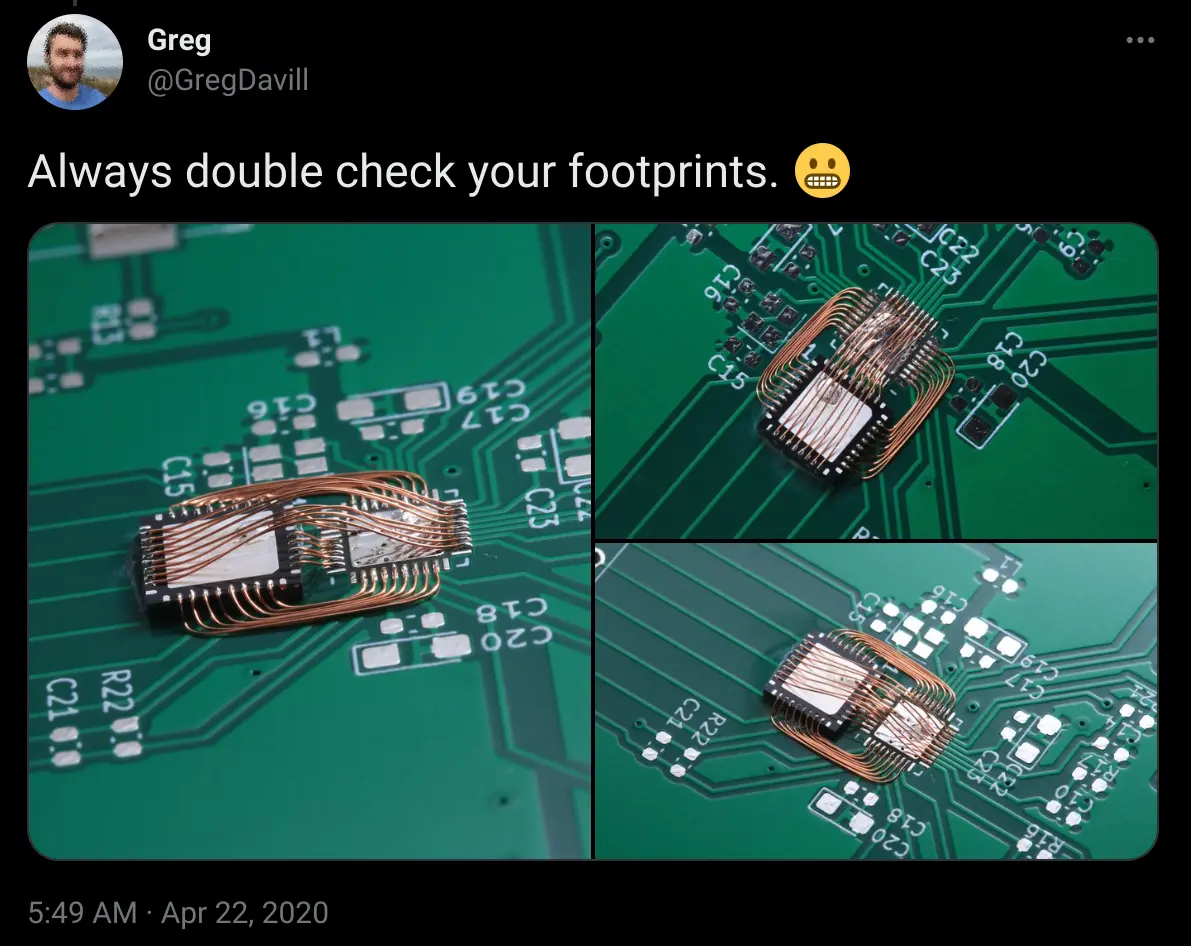
Tweet from @GregDavill

Let KiCad and Python design your PCB Coils [Hackaday]
KiCad STM32 + RF + USB Hardware Design (YouTube, Phil’s Lab)
https://hackaday.io/project/174310-copxie-chainable-dual-57-tiny-led-matrix
Chapter 26.1 - PCB Components #
It turns out that there’s quite a few components which you can make into the PCB itself, basically costing no more than the price for the extra area on the PCB.
Probably the most common of these to see is antennas, usually for 2.4Ghz (WiFi and Bluetooth). These require some pretty gnarly math to design and make actually compliant with radio frequency regulations, but they’re still pretty sweet.
[TODO] picture
You’ll also ocassionally see PCB Spark gaps (EEVblog, YouTube) which are useful for protecting againt high voltage spikes. Similarly, it’s possible to make a fuse by using a very thin trace. See This video by Leaf Rex (YouTube)
It’s also possible to impliment coils, useful for inductive coupling or transformers - see RGB LED, Inductively Powered, Frequency Controlled (Wolf Tronix, YouTube).
Getting a bit weirder, you can also make a capacitor by using traces on different layers; however, you’ll usually only be able to get up to a few hundred pico ferrads max. It’s typically not worth the complexity introduced, espically as the exact value will be variable due to manufacturing tollerances.
Entering the relm of black magic fuckery, you can actually make high frequency filters by adjusting the length and gaps between traces - these are called distributed element filters and are really fucking cool.
Finally, I want to mention that there’s some pretty esoteric PCB manufacturing methods, though the weirder you want, the more you pay. For example, making PCBs with Heavy copper traces (Hackaday) is totally possible, but you’ll pay for it.
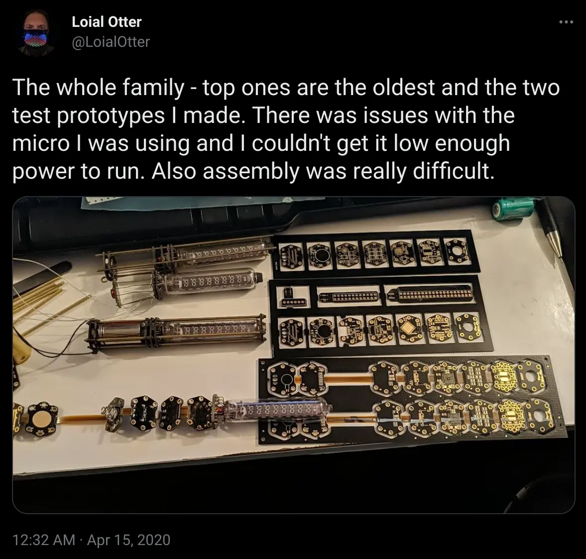
Chapter 26.2 - Pretty Boards & Badges #
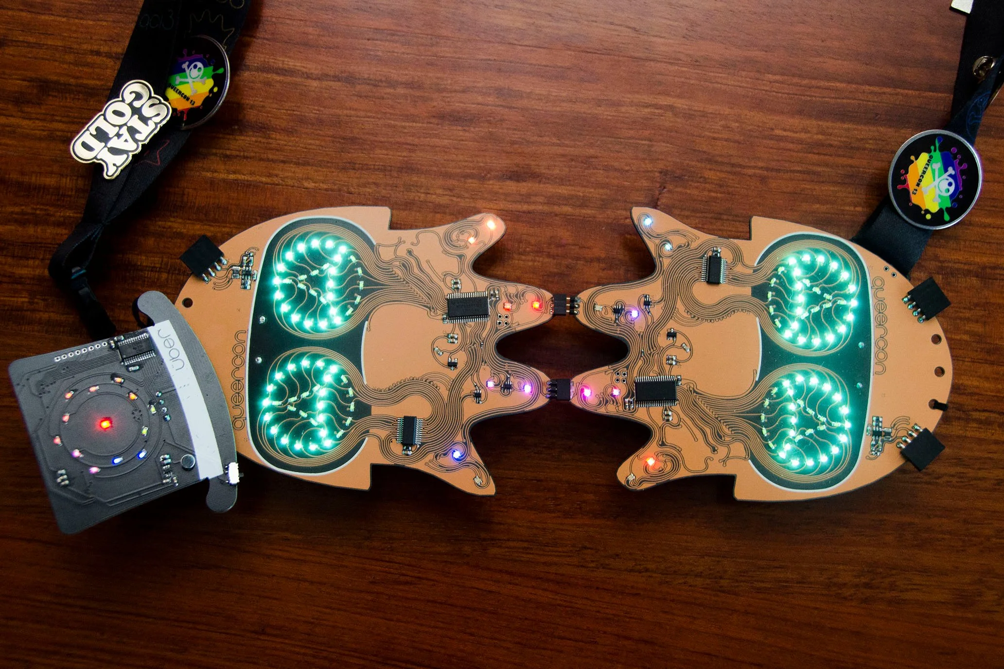
Source: @AkioOhtori on Twitter
https://hackaday.com/2018/08/21/all-the-badges-of-def-con-26-vol-2/
Furby Theremin Badge (Tindie, Harbinger LTD)
https://github.com/badgeek/svg2shenzhen
https://mitxela.com/projects/melting_kicad
OSH Park After Dark - Clear Solder Mask
Chapter 26.3 - Alternatives to PCBs #
[TODO] Wirewrap, permaproto, etc.