3 - The Motherboard #
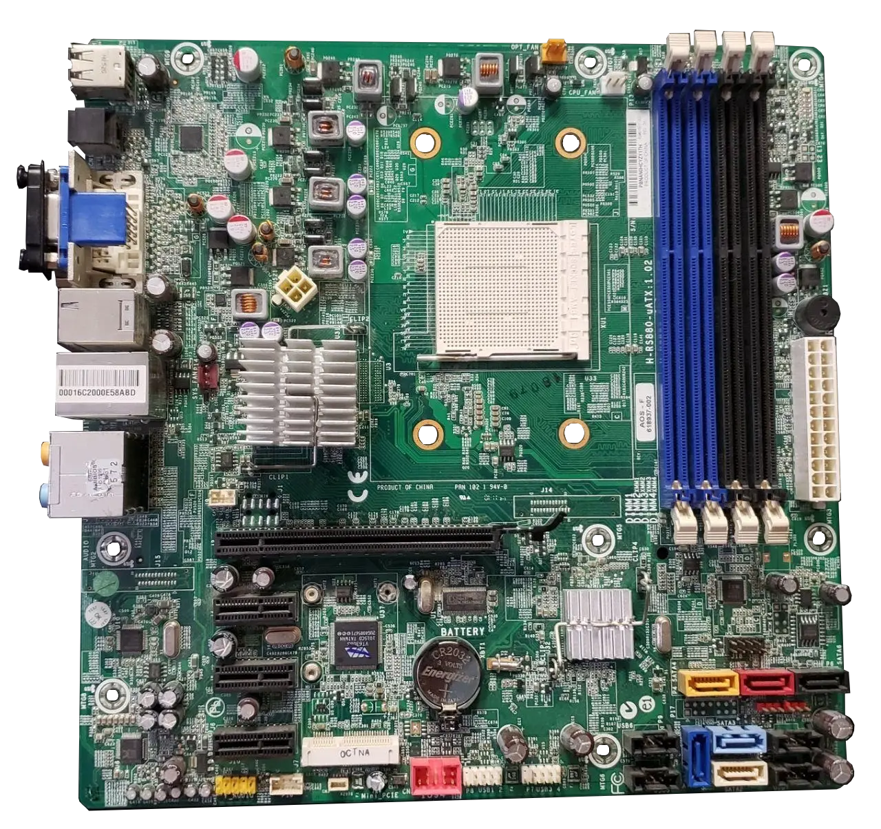
This is an older motherboard, but still new enough to have modern parts. Let’s start by looking at the most obvious physical features and move to smaller things from there.
The most obvious thing to point out is the size of the motherboard. This is a mATX motherboard, which is considered the normal size for most systems. Most gaming or DIY computers will use full size ATX motherboards, which look very similar but are a bit longer vertically, allowing for more expansion slots - those horizontal black bars - among other features. Other form factors include ITX, a smaller form factor with only a single expansion slot, eATX (extended ATX) which is rarely used now, and SSI and EEB which are both server motherboard sizes.
The large, white square is the CPU socket. This is an older board made for an AM3+ processor. The AM3+ processor line, as well as most consumer processors from AMD use a PGA or Pin Grid Array socket. these CPUs have many pins on the bottom which fall into these holes to make contact. Before the CPU is inserted the metal leaver arm, seen at the bottom of the socket if you look carefully, is raised and the CPU should smoothly plop right in, after which the arm can be lowered. Modern Intel CPUs follow a similar-ish mechanism, only instead of having a bunch of pins that go into holes the ‘pins’ are actually tiny springy pieces of metal on the motherboard which make contact with pads on the CPU, that socket looks a bit like this, albeit this is an old one:
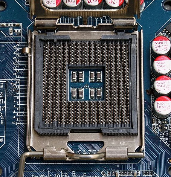
Image By Appaloosa, Own work , CC BY-SA 3.0, Wikipedia Image Link
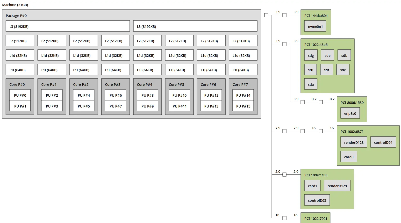
If you’re looking at a server or high end workstation you may actually run into a single motherboard with multiple CPU sockets. These are becoming less common with time, but even though there are multiple CPUs the system still operates as one larger system. For example, I have access to a system with 4, 8 core, 16 thread cpu’s to give for a total of 64 threads. Giving this beautiful sight:
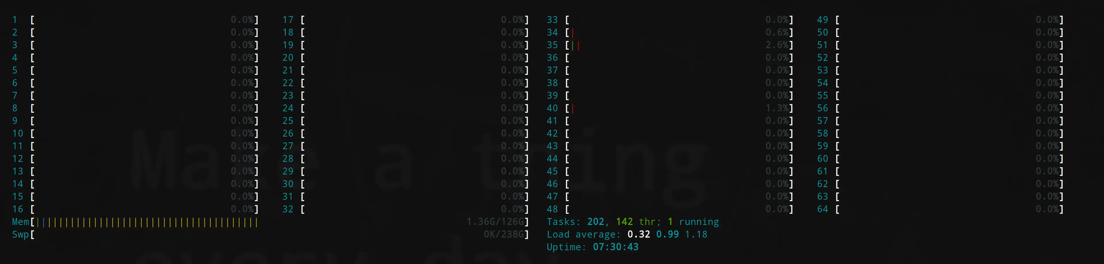
Clearly, a server with that much horsepower will use a lot of electricity though, and there is some overhead for the system when getting information from one physical CPU to another.
Above and left of the CPU on you’ll see a bunch of copper coils in little boxes and some small metal cylinders, as well as a cluster of these with a large, 4-hole plug a bit further left, directly above the big aluminum heat sink. This all makes up the VRM or Voltage Regulation Module. The connector there is where the CPU power plug from the PC power supply would be plugged in. The power needs to be carefully controlled, filtered, and adjusted based on the needs of the CPU, that’s what all of this is for. Generally the beefier and faster a CPU, the larger the VRM. The VRM also needs to dissipate a good amount of heat on higher end systems so many nicer motherboards will cover this up with a large heatsink.
Moving on from the CPU you’ll see 4 vertical slots next to socket, these are where the RAM sticks are inserted. You’ll notice they’re color coded as to indicate which slots share the communication channel, so in this case you’d want to put the first memory stick in the blue slot closest to the socket, followed by the black slot closest to the socket, then repeat.
While we’re looking at this side of the board- next to the RAM slots you’ll see two things of note. First, that black circular thing is actually a little buzzer. A lot of even modern systems have these on board to buzz error codes out in morse code if something goes wrong. Below that is a large, 20 or 24 pin connector (most modern systems use the 24pin varient) which is where the power supply is plugged in to provide power to the motherboard (with the exception of the CPU) as well.
On the other side of the CPU and down a little you’ll see a sizable metal heatsink. This is covering the chipset. We’ll come back to what the chipset does in a bit. This motherboard is actually a bit weird, on most motherboards the chipset is found almost directly below the RAM, but in general look for a large heatsink and it’s probably under that.
Below the chipset here are 4 expansion slots, all of which use the PCI-e standard in this case. We’ll come back to these in a bit.
In the bottom right of the motherboard there are 6 SATA connectors, here each is a different color (for no apparent reason?). These are for connecting storage like hard drives.
Vertically in line but closer to the center of the board you’ll also spot a coin cell battery. This is so the system can keep time with use of an on board Real Time Clock (RTC) even when fully powered down and disconnected from wall power.
Along the bottom you’ll see various connectors with pins sticking out, these are mostly for front panel connections- where the USB, audio, power button, etc. from the front of your case connect.
Finally, along the top of the back left edge you’ll see the metal tops of the main ‘rear i/o’ for the computer. These are all the main connections for your system. The bulk of the system’s USB ports, networking, and audio ports will be found here.
So, how do we get any information from the motherboard? Well, in case it wasn’t already obvious, the motherboard isn’t really one thing. It’s more a common interconnect point and routing system than anything; however, it does have some of it’s own responsibilities. To start small let’s look at one small, but exceedingly import role of the motherboard: fan and temperature control.
To see what your fans are doing on Linux you’ll need to grab the package lm_sensors with yay, then you can run sudo sensors-decect and mash enter until it’s done. After this you should be able to run sensors and see an output similar to this one:
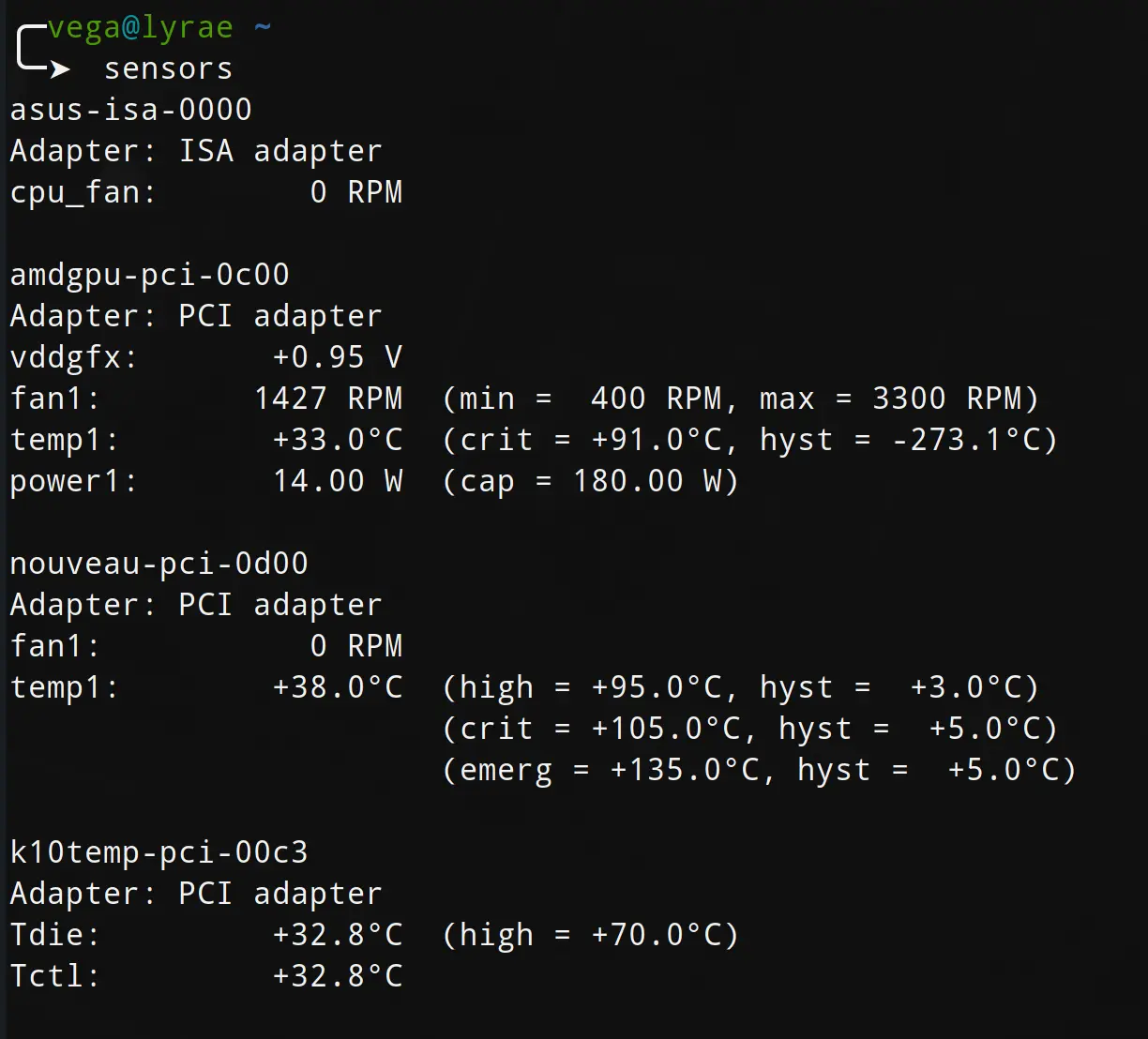
Of note, depending on your system, there’s a small chance nothing will be detected at all or that some information will be wrong. Even in my case this is true as my CPU fan is reporting 0 RPM. Actually entering your motherboard’s UEFI or BIOS settings may expose more information, but we’ll talk about that more later.
Alright, so that’s coll and all, but what else can you do?
Alright, let’s move on to seeing the system buses, namely, the pci bus.
The pci bus is where most of the system’s add in cards, controllers, and the like connect. Here’s a shortened version of the output of lspci from my system
|
|
Alright, clearly there’s a lot going on here, and on first glance it doesn’t even look all that useful. But let’s look deeper. From this output we can see some interesting things. Starting from the top you’ll see there’s a lot of internal AMD things that are just handling routing, really these probably don’t matter. the first interesting things to look at is 01:00.0 Non-Volatile memory controller: Phison Electronics Corporation E12 NVMe Controller (rev 01) which is telling me that my super speedy NVMe solid state drive is at the address 01:00.0 on the pci bus and despite being made by a consumer brand (I think mine’s a Silicon Power? though I have another that’s made by Samsung) the actual controller on the device is made by Phison, a reputable brand for NVMe controllers.
next thing of note is
|
|
You can see here that I have a separate controller for my USB 3.1 ports and that it’s sharing pci lanes with my sata controller. In theory, this means If I’m working one or both of these really hard, the other may be slower.
next is:
|
|
What’s interesting here is I have another 3.1 controller, on an entirely different set of lanes. Really, this is a fault of USB that it’s not very clear, this is actually a USB 3.1 gen 2 controller, so each port has a top speed of 10gb/s, compared to the 5gb/s of the other controller.
You’ll also see that my network interface is being handled by an Intel network controller, despite this system having an AMD CPU.
moving on:
|
|
Here you’ll see some devices can actually use multiple IDs for one physical device. both of the 0c:00.x ‘devices’ are actually for the ‘Vega56’ graphics card (Often called GPU for graphics processing unit) made by AMD Radeon, while the 0d:00.x devices are for the GTX1060 card made by Nvida that I have in this system as well. Of note, having both of these in one system is exceedingly uncommon, and my use case is strange; however, It is common to see systems which have a gpu integrated into the CPU (which will still appear in this list) and have a separate larger GPU in the system as well.
If you continue down this list you’ll see there’s yet another USB controller and a audio controller among other things.
What’s cool is this information relates back to something we saw earlier when looking at the CPU:
See all those PCI ids on the right side, those directly correlate with a lot of the above.
Finally, if you want a lot more information you can run sudo lspci -v to see even more info about anything, for example, here’s the output about my GTX1060 GPU:
|
|
The most notable thing here is actually at the end:
|
|
tells us I’m using the nouveau driver and kernel modules instead of one of the alternatives on the Nvida card in my system If I wanted to I could switch this over to the proprietary Nvidia driver to get a pretty nice speed boost in some applications.
I’m not really worried about this because I’m mostly just using the Vega56 card. The nvidia card is there strictly for CUDA support in some workloads.
Much like lspci, there’s also lsusb, which as you can imagine, tells us information about the USB devices on the system. I have a LOT of usb devices on this system so I’ll just paste in a snippet:
|
|
You’ll see here that USB hubs, input devices, webcams, etc. all show up. Anything that’s hooked up through USB should appear here. The device with ID 258a:0013 isn’t really telling us anything though. What we do know is the first part is the USB Vendor ID. This is an ID that vendors of USB devices have to purchase to uniquely id their products.
upon looking this id up online, it appears it’s used for a generic USB keyboard.
For completeness I’ll mention, the first part of the id, the x’s in xxxx:yyyy is the vendor id, while the y’s are the product id.
Finally, I’d like to mention dmidecode. according to the manual page:
dmidecode is a tool for dumping a computer’s DMI (some say SMBIOS) table contents in a human-readable format. This table contains a description of the system’s hardwarecomponents, as well as other useful pieces of information such as serial numbers and BIOS revision. Thanks to this table, you can retrieve this information without having to probe for the actual hardware. While this is a good point in terms of report speed and safeness, this also makes the presented information possibly unreliable.
we’ve already used this to get information about the system ram, but other things can be read as well. For example, going back to the pci slots from above running sudo dmidecode --type 9 will tell you what physical slots correspond to what bus address among other information, for a full list of available types simply look at the dmidecode man page with man dmidecode.
Chipset #
The chipset is a chip usually located in the bottom right 1/4 of a motherboard underneath a heatsink. The chipset coordinates the data flow between the processor and most of everything else- excluding the few direct-CPU attached things like the Graphics card. Older systems had both a Northbridge and a SouthBridge as two separate chips, but everything modern has just the single chip, as the Northbridge, which had memory the memory controller, isn’t necessary on modern systems where the memory controller has been integrated into the CPU itself.
For the most part, the chipset on a motherboard will match a certain CPU socket, that is each generation of CPU will have it’s own chipset and socket; however, this is not always the case as sometimes one chipset may support multiple CPU generations or a CPU generation will work with multiple chipsets. This is the case with AMD’s ryzen line where a first generation Ryzen CPU such as the Ryzen 1700 will work in a motherboard with an x370, x470, or x570 chipset, and a third generation Ryzen CPU such as the Ryzen 3700 will work in any motherboard with one of those as well, albeit running a generation mis-match may result in degraded performance or missing features (such as lacking PCIe 4.0).
Finally, it’s notable that the chipset typically acts as a PCIe lane ‘splitter’ of sorts, turning (usually) 4 lanes into may more so that more devices may be attached. This can be particularly important when many high bandwidth devices are attached though, as even though these lanes are split, there’s still only that original 4 lanes of bandwidth to go around.
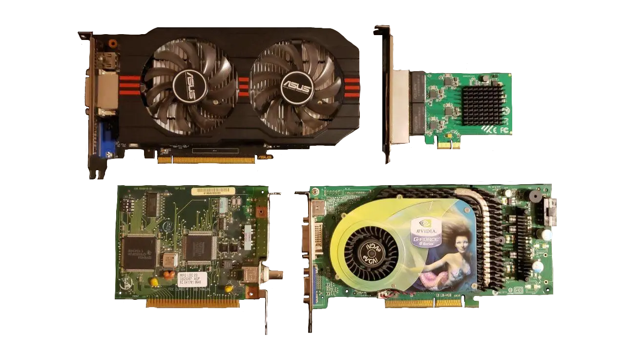
Expansion slots #
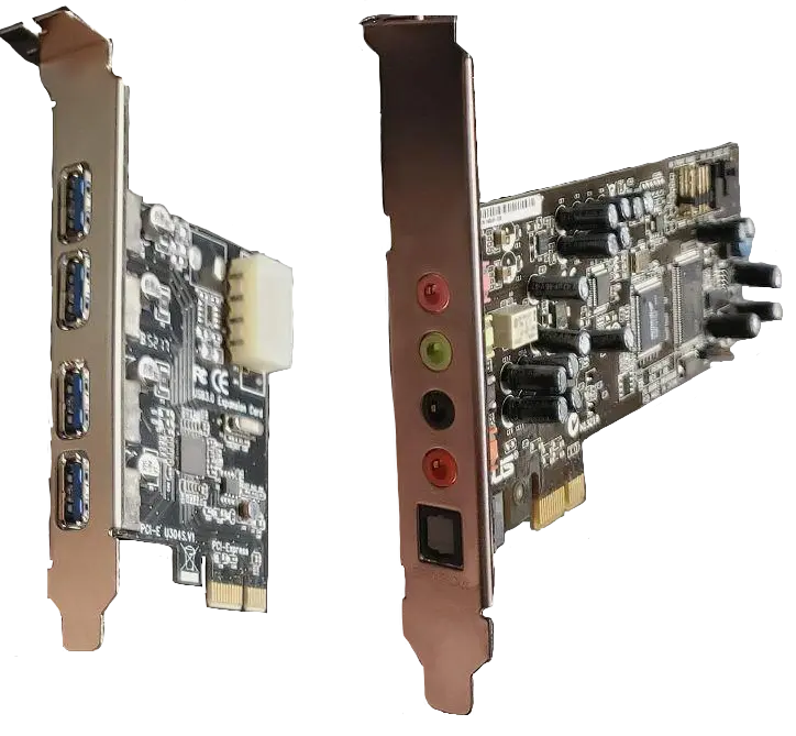 Two PCI-e 1x expansion cards, one for USB 3.0 and one for audio. Of note, most modern motherboards have both functions built in.
Most modern expansion cards connect though the PCI Express or PCIe bus. This standard, much like DDR, has gone though multiple generations of bandwidth doubling. Currently consumer devices offer up to PCIe 3.0 but devices with both 4.0 and 5.0 should be on the market shortly.
PCIe cards are used for just about anything you could imagine, form adding a more powerful graphics card, more usb ports, a higher end sound card, to some more esoteric things like specific task accelerators (encryption, compression) or even a software defined radio.
No matter what the device is you have to keep in mind its physical and electrical requirements. That is, do you have a slot long enough to accommodate the card and can you provide power to it.
This may seem odd, but unlike most connections (think USB or Ethernet) which may support varying speeds (usb2 vs 3) but are still physically the same size, the more bandwidth hungry a PCIe device, the larger the physical connection. The largest available is a 16x connection, while the smallest is a 1x. The most commonly used lane arrangements are 1x, 4x 8x, and 16x. The motherboard shown above has one 16x connector and three 1x connectors. If you have a card that is electrically wired for 4x it will definitly work in any slot physically designed for 4x or greater, and it will still work in a 1x slot of that slot is open ended- this means the ‘back’ of the slot is open, allowing the card’s connector to go past the actual physical connection. Similarly, many 16x physical slots only have 8x actually wired. If you use a card which elecrically needs more connections it will almost certainly still work, but may have degraded performance. Similarly, if you have a card which expects a PCIe gen 3 16x connection but the best you have available is a PCIe gen 2 connection, it will run at half speed. To be extra clear:
PCIe 1 @ 16x == PCIe 2 @ 8x == PCIe 3 @ 4x
Similarly, putting a card which only supports PCIe Gen 2 into a Gen 3 slot will not suddenly make the card faster, even if it was to compensate, that is, if the card is made for PCIe Gen 2 @ 16x and you put it in a PCIe Gen 3 @ 8x slot, it will still run at half speed because it’s the lowest gen number of the card or the slot that determines how many lanes are actually needed.
Unfortunately, PCIe lanes, that is if you add together all the available 16x’s and 8x’s etc. on a given CPU are usually pretty limited. If the only extra card you plan on adding is a graphics card, you’ll be fine, but if you intend to add a graphics card, sound card, network card, etc. all at once you may find that you’ve either run out of physical slots or that a card is running with less than ideal bandwidth as a 16x slot may ‘give up’ 8 of it’s lanes becoming an 8x slot so that another card can function at all.
Of note, the number of physical lanes and slots the mother board has probably greatly exceeds the number of lanes actually going to the CPU, so even if it appears you have plenty of room to add cards you may end up accidentally starving one for bandwidth.
Finally, from a power perspective most motherboards will supply up to 75 watts to a card through the motherboard, but power hungry cards like the Nvidia and AMD graphics cards in my system may require external power connections. Also, some server boards cap PCIe power delivery to only 25 watts without an external power supply, so just be careful with compatibility.
There are some other standards other than PCIe worth mentioning though.
Older standards such as PCI, AGP, and ISA were all used before the widespread adoption of PCIe and while their availability is declining, PCI cards are still often for sale, you need to be very careful to only get PCIe cards and not PCI cards if your system doesn’t support them.
Both AGP and ISA have been phased out a long time ago, but very old cards may poke up now and then. If you’re into vintage computers you may want to look the standards up to learn more.
Top: a 16x pci-e graphics card and a 1x pcie networking card
Bottom: an ISA networking card and an AGP graphics card, not pictured is the PCI connector
ROM/BIOS/UEFI #
Motherboards have to coordinate the communication of all the peripherals on the system and their own internal buses, furthermore, they have to have some sort of minimal configuration settings for setting things like which drive to boot off of or what speed the CPU or RAM should run at. These configuration settings are stored in some ROM or ‘Read Only Memory’, which is an independent chip on the motherboard. This configuration is read by the Binary Input Output System (BIOS) or the Unified Extensible Firmware Interface (UEFI). UEFI is essentially just the newer replacement for BIOS, and usually includes a compatibility mode for BIOS based hardware. When you first turn on the system you can typically mash either the delete or F12 key to enter this configuration page. It’s typically from this interface that you’d select your boot device, change your CPU or RAM clock speed, and set the system time. On that note, the system also likely has a battery on board which power’s the on-board real time clock, which allows the system to maintain the time even when disconnected from power. On some systems the ROM is actually volatile meaning if this battery dies and the system is disconnected from power you may loose the BIOS/UEFI settings.
Of note, you may need to update the UEFI or BIOS of a system which is sometimes done via a special admin command within windows but more commonly done by downloading a file to flash drive, putting the drive in a specific usb port, and loading the update file. When this is done it’s common to lose all UEFI/BIOS settings as well, as it overwrites the ROM.
Finally, it should be noted that it’s pretty easy to make your system not boot or boot-loop if you break things here. So, be careful. If you set your fan speeds slower to make the system quieter then everything overheats and dies, well, ヽ(´ー`)┌
Because this varies per motherboard there’s no universal way to describe how it looks or works. Some boards will support a lot more configuration than others, with really the only nearly definite options you’ll find at the time of writing being a switch to enable virtualization extensions (for running virtual machines) and a switch to turn of Secure Boot, which you likely had to do to install Arch to begin with.
Further reading: How To Geek: What Is UEFI, and How Is It Different from BIOS? , UEFI and why I Hate it so Much (Cheapskate’s Guide)
VRM #
The VRM or ‘Voltage Regulation Module’ serves a simple but important task of ensuring that the CPU (or processor in question) receives a constant voltage or voltage that makes sense for it’s current clock speed.
Essentially the VRM may contain multiple stages of current and voltage regulation modules. The more of these stages the more stable the voltage and the more current can be delivered. For most cases, this can be left alone, but it’s incredibly important when over clocking, as to overclock a CPU or GPU it’s usually necessary to increase the voltage, which is typically done from within the BIOS/UEFI or from a configuration utility inside the OS in the case of the GPU.
You can typically tell how strong a particular uVRM is by counting the number of ‘chokes’ on the board.
[TODO, add pictures of chokes]
TPM #
[TODO]